High Temperature Superconductors (HTS) can impact a broad spectrum of sectors of the US economy such as energy, defense, industrial applications, communications, and medicine. In the energy sector, for example, HTS devices have the potential to benefit both renewable and non-renewable energy industries, accelerate introduction of smart grid hardware applications and improve sustainability through enhanced energy efficiency, high power density, less CO2 emission, better power quality and improved resiliency and security of the power grid. Superconducting devices do not simply provide improvements over conventional technologies; they provide unique solutions to challenges that cannot be achieved otherwise.
High Temperature Superconductors Enable Clean Energy Future
Since superconductors are typically used in presence of a magnetic field, their critical current performance in a magnetic field is an important metric. In a thin film superconductor tape without any added dopants, the critical current density at 77 K decreases by a factor of 7 to 10 when a magnetic field of 1 T is applied perpendicular to the tape plane. At the University of Houston, we have employed heavy doping (15% – 25%) of Zr to form a high density (1011 – 1012 cm-2) of BaZrO3 (BZO) nanoscale defects in the thin film superconductor matrix to pin the magnetic flux lines and achieve substantially improved critical current in high magnetic fields. The BZO defects are formed by a self-assembly process simultaneously during the epitaxial growth of the REBCO film. In a program funded by the Advanced Research Projects Agency-Energy (ARPA-e), we successfully developed a Metal Organic Chemical Vapor Deposition (MOCVD) process to achieve a high density of well-aligned BZO nanocolumns in heavily-doped REBCO films (up to 25 mol% doping) while maintaining excellent epitaxial growth [1].


Microstructures of a 25 mol.% Zr-doped thin film superconductor film synthesized by MOCVD showing abundant columnar structures of self-assembled BaZrO3.
By this process, we were able to improve the critical current of REBCO tapes by three-fold in high magnetic fields at 30 K. Record-high critical current density above 20 MA/cm2 at 30 K, 3 T [2] and pinning force levels above 1.7 TN/m3 [3] have been achieved in heavily-doped REBCO thin film superconductor tapes.
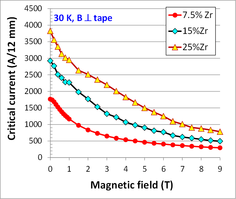

(Left) Improved critical current of thin film superconductor tapes at 30 K, 3 T with increasing levels Zr addition. (Right) Flux pinning force levels of thin film superconductor tapes made by institutions world-wide. Courtesy T. Puig, EUCAS 2015
We are working towards consistently achieving a high density of highly-aligned nanoscale defects over long tape lengths. The film composition and lattice parameter of the REBCO film and BZO nanoscale defects have been found to be key parameters in determining the alignment of the defects and hence the in-field critical current performance. In-line quality control tools such as X-ray Diffraction are being developed for real-time monitoring of the REBCO film characteristics to achieve a consistent nanoscale defect microstructure and in turn a consistent in-field critical current over long tape lengths.
Advanced Metal Organic Chemical Vapor Deposition (MOCVD) process for high performance thick film superconductor tapes
A challenge with achieving high critical current is the reduction in critical current density with thickness of the superconducting layer. We are working on improving critical current performance levels in thick films by addressing current-limiting mechanisms in superconducting films deposited by metal organic chemical vapor deposition (MOCVD). A main current-limiting mechanism is the increased growth of misoriented a-axis grains and deterioration of epitaxy in films thicker than 2 µm. This problem stems from inadequate temperature control during growth of thick films. The temperature control is even more critical in growth of thick films with high levels of dopant that is used for flux pinning.
 Thickness dependence of critical current density of thin film superconductor tape. The critical current density decreases and the critical current begins to saturate in thicker films

Deterioration in microstructure of thin film superconductor tape beyond 2 µm with the formation of misoriented a-axis grains. These grains are also seen as (200) peaks in the X-ray Diffraction data
We have developed an Advanced MOCVD reactor to address the challenges in growth of high-quality thick superconductor films [4]. Rather than a using a heater, the tapes are heated directly by ohmic heating wherein current is flowed directly into the tapes making use of the high resistivity of the Hastelloy substrate. Eliminating the heater also allows access to directly monitoring the temperature of the tapes using optical probes. Using the Advanced MOCVD system, 4 – 5 µm thick films have been growth with essentially no a-axis grains. Critical currents as high as 1600 A/12 mm have been achieved in these films, which is about 50% higher than that previously obtained in films grown in conventional MOCVD reactor [4].


(Above) Schematic of Advanced MOCVD reactor. (Below) Surface and cross sectional microstructure of thick film REBCO films made by Advanced MOCVD
The Advanced MOCVD reactor also has other new features such as a laminar flow channel which enables a high efficiency in the conversion of expensive metal organic precursors to film. This is especially important since only 10% of the precursors are converted to film in a conventional MOCVD reactor and the precursors are the most expensive component of the overall wire cost. High precursor conversion efficiency also leads to high throughput which is important for high-volume manufacturing. We used the Advanced MOCVD reactor to fabricate 4 – 5 µm thick REBCO films with record high critical current over 8700 A/12 mm at 30 K, 3 T [5] which is about seven times higher than the performance of commercial HTS tapes. The engineering current density of the thick film REBCO tapes made by the Advanced MOCVD method is about 5.5 kA/mm2 at 4.2 K, 14 T [6] which is over 5 times higher than the best reported performance of Nb3Sn superconductors which is the primary superconductor used now in high-field applications.
We have successfully fabricated 4 µm thick film REBCO tapes using Advanced MOCVD with excellent critical current performance. REBCO tapes with 4 µm thick films and 5% Zr addition exhibit critical currents of 1285 A/cm which is a factor of 4 higher than the performance of the best commercially-available REBCO tapes.
 Critical current of GdYBCO tapes with 4 µm thick films and 5-15% Zr addition at 65 K, 1.5 T made in the program funded by the DOE- Advanced Manufacturing Office (AMO). The performance of the best commercially-available REBCO tape is included for comparison.
As the following figure shows, the engineering current density (Je) of UH REBCO tapes is 5.4 times the Je of Nb 3 Sn at 4.2 K, 15 T. The critical current (Ic) of UH REBCO tapes developed in our DOE-HEP program, at 4.2 K, 18 T is 1836 A/4mm-width [4] (Figure 2) which is >3x the Ic of the best commercial tapes at 18 T by Faraday Factory [5] by Pulsed Laser deposition (PLD) and by SuperPower [6] by MOCVD.
 Engineering current density of UH REBCO tapes in high magnetic fields at 4.2 K, compared to other superconductor technologies (other data from National MagLab).

Performance of University of Houston’s REBCO tapes at 4.2 K in magnetic fields up to 31 T in comparison with the best commercial REBCO tapes [5, 6].
New In-line Metrology Tools
In order to scale up REBCO tapes with the excellent high-field performance demonstrated in Figures 1 and 2 to manufacturing, consistency and uniformity in Ic have to be achieved. Measurements of commercial tapes showed a factor of 3 variation in Ic in high magnetic fields at 4.2 K and 20 K for the same Ic at 77 K, 0 T [7, 5]. REBCO tapes are especially prone to non-uniformity and inconsistency because of the sensitivity of in-field Ic to the film composition and nanoscale defect structure. As shown in Figure 3, the superior Ic of our tapes at 4.2 K, 13 T is achieved in a narrow range of film composition (~ 1 at.%). This data was obtained by inductively-coupled plasma spectroscopy (ICP) – a destructive measurement. In order to control the film composition of long tapes within a narrow range, non-destructive measurement of the film composition is needed – one that can be implemented for real-time assessment during tape fabrication.

Figure 3. Compositional map showing REBCO compositions that yield the highest Ic at 4.2 K, 13 T.
In our ongoing DOE-HEP program, we have developed such a measurement method, based on 2D-X-ray Diffraction (XRD) for rapid assessment of the film composition. This method is based on our discovery that with increasing Ba composition in the film – as represented by the metric (Ba+Zr)/Cu, the c-axis lattice parameter of film increases and the lattice parameter of BaZrO3 (BZO) decreases (Figure 4a). Building on this finding, we observed in a 2D-XRD scan, the distance between REBCO (103) and BZO (101) peaks decrease with increasing Ba content which is manifested as a decrease in streak angle between the BZO (101) streaking direction and normal to the (00l) axis (Figure 4b). As shown in Figure 4c, the BZO (101) streak angle measured by 2D-XRD is a strong predictor of the film composition in terms of (Ba+Zr)/Cu and the Ic at 4.2 K, 13 T. In essence, films with low values of BZO (101) streak angle are reflective of high levels of (Ba+Zr)/Cu and high Ic in high fields at 4.2 K. This important discovery enables us to assess the film composition of our tapes non-destructively by 2D-XRD in real time during film growth. This can help maintain the film composition in a narrow compositional window shown in Figure 3 to obtain consistent and uniform high Ic in long tapes, close to the levels demonstrated in short samples in Figures 1 and 2.


(a) (b) (c)
Figure 4. (a) C-axis lattice parameter of REBCO film and BaZrO3 in films with increasing content of Ba, as measured by high-resolution X-ray Diffraction of Zr-added REBCO tapes. (b) 2D-XRD scans showing REBCO (103) and BZO (101) peaks of REBCO tapes with normal Ba and high Ba content. The BZO (101) peak of the sample with normal Ba streaks in the 2-theta direction whereas the BZO (101) peak of the sample with high Ba streaks normal to the (00l) axis. The (00l) axis is along the horizontal direction (χ = 0°) in 2D-XRD scan. (c) Relationship among film composition in terms of (Ba+Zr)/Cu, magnetization Ic at 4.2 K, 13 T and BZO (101) streak angle measured by 2D-XRD of Zr-added REBCO tapes with different Ba content
We have implemented an in-line 2D-XRD in our A-MOCVD process to monitor the film composition and BaMO3 (BMO) nanoscale defects during tape fabrication [8]. Figure 5 is a photograph of our A-MOCVD tool with inline 2D-XRD enclosure at the right of the reactor. A close-up view of the tape path, X-ray source and 2D-XRD detector positioned in line with tape motion is also shown. Figure 5 summarizes the results of an inline 2D-XRD scan of a 10-m tape made by A-MOCVD, showing the variation in individual peak intensities. In addition to the raw intensities used to calculate changes in structure factor resulting from compositional variation, many other parameters are extracted from the scan: BZO streak angle, lattice parameters, texture and secondary phase content, as a function of process conditions.


Figure 5. (Left) Photograph of A-MOCVD tool with inline 2D-XRD. (Center) View of the tape path, x-ray source and 2D-XRD detector. (Right) Integrated intensities of REBCO (003), (005), (103), BZO (101) and REO (400) peaks obtained from 2D-XRD scan of 10-m-long REBCO film in real-time during film deposition.
This abundant real-time data from in-line 2D-XRD can be used to to take corrective actions during tape fabrication to assure uniform film composition.
Advanced Practical 2G HTS wire
eyond critical current, in-field performance, lower cost and higher manufacturing throughput, it is important to develop superconductors which can meet other application requirements such as low AC losses, quench stability, robust mechanical properties, persistent joints, fault current limitation and recovery to name a few. Reduction in ac losses requires low hysteretic, eddy current, and coupling losses. Hysteretic losses can be minimized by subdividing the superconductor into fine filaments. At UH, we are working on dry etch and wet etch techniques to create multifilamentary 2G HTS wire architectures that lead to reduction in ac losses.


Multifilamentary second-generation high temperature superconducting tape and lower ac losses
We have developed a laser striation and a selective electroplating process to fabricate fully-stabilized multifilamentary thin film REBCO superconductor tapes. Every superconductor filament of these tapes is individually encapsulated with a copper stabilizer which provides the benefit of cryostabilization along with low AC losses. 10 – 20 m long tapes have been made with 12 filaments, 24 filaments and 46 filaments [9] as shown in the following figure. The filament integrity was maintained uniformly over the long lengths. The copper electrodeposition was confined on the filaments without coupling between them.


Photographs of multifilamentary REBCO tapes made by laser striation followed by selective electroplating. (top-left) 12 filaments (top-right) 24 filaments (bottom-left) 46 filaments (bottom-right) 46 filaments after copper deposition
AC loss measurements at 100 Hz in AC fields up to 80 mT conducted on the 12, 24 and 46 filament tapes and a reference non-striated tape show that AC losses reduce proportional to the number of filaments in the tape. No evidence of coupling between the filaments was found.
 AC loss measurements on 12, 24 and 46 filament REBCO tapes made by laser striation and a non-striated reference tape.
Multi-strand REBCO wire architectures:
A challenge with REBCO tapes as compared to Nb-Ti, Nb3Sn and Bi-2212 wires is their flat rather than round geometry and a wide (~ 12 mm) profile rather than a multifilamentary architecture. A round REBCO wire can be mechanically isotropic in bending which can benefit several conductor and magnet designs especially those using canted cosine theta (CCT) coils. If the minimum bend radius of such a round REBCO wire can be reduced to 15 mm, the tilt angle in winding the CCT coils can be lowered to 30o and the dipole transfer function can be nearly doubled to 0.48 T/kA with a four-layer design and to 0.73T/kA with a six-layer design [10]. To greatly improve the bend tolerance, UH and its industrial partner AMPeers developed a symmetric tape architecture that places the REBCO film near the neutral plane which renders it very tolerant to bend strain. Symmetric REBCO tapes can be bent to 0.8 mm in diameter with greater than 95% Ic retention. Utilizing this new type of tape, UH and AMPeers have demonstrated symmetric tape round (STAR®) wires of 1.3 – 3 mm in diameter that exhibit exemplary electromechanical properties [11]. STAR® wires have also made with high Ic Advanced MOCVD REBCO tape strands, confirming that even tapes with 4-5-µm-thick films can be wound onto very small diameters if made in a symmetric format. Je values of nearly 600 A/mm^2 have been achieved at 4.2 K, 30 T in STAR® wires made with Advanced MOCVD tape strands [12]. STAR® wires have been to demonstrate prototype CCT magnets [13], Conductor-on-Molded-Barrel (COMB) magnets [14], and 6-around-1 cables [15].
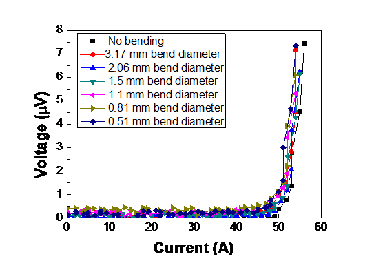 Current-voltage (I-V) curves of 2 mm wide, 25 µm ultra-thin symmetric REBCO tape when tested in a bent state over formers of different diameters. No degradation is observed in critical current even at a bend diameter of 0.51 mm!


(Left) Photograph of an 1.6 mm diameter round REBCO wire made by spiral winding six layers of 45 µm thick tapes over a 0.81 mm diameter former. (Right) Photograph of the round wire after bent to a diameter of 3 cm.
 Magnetic field dependence of Je of the REBCO STAR Wire-2 at 4.2 K.
References :
V. Selvamanickam, M. Heydari Gharahcheshmeh, A. Xu, Y. Zhang and E. Galstyan, , Supercond. Sci. Technol. 28, 072002 (2015).
- V. Selvamanickam, M. Heydari Gharahcheshmeh, A. Xu, E. Galstyan, L. Delgado and C. Cantoni, “High critical currents in heavily doped (Gd,Y)Ba2Cu3Ox superconductor tapes”, Appl. Phys. Lett. 106, 032601 (2015).
- A. Xu, N. Khatri, Y. Liu, G. Majkic, V. Selvamanickam, D. Abraimov, J. Jaroszynski and D. Larbalestier, “Broad temperature pinning study of 15 mol.% Zr-added (Gd, Y)-Ba-Cu-O MOCVD coated conductors”, IEEE Trans. Appl. Supercond. 25, 6603105 (2015).
- G. Majkic, E. Galstyan and V. Selvamanickam, “High Performance 2G-HTS Wire Using a Novel MOCVD System”, IEEE Trans. Appl. Supercond. 25, 6605304 (2015)
- G. Majkic, R. Pratap, A. Xu, E. Galstyan, H. C. Higley, S. O. Prestemon, X. Wang, D. Abraimov, J. Jaroszynski and V Selvamanickam, “Engineering Current Density over 5 kA/mm2 at 4.2 K, 14 T in Thick Film REBCO Tapes”, Supercond. Sci. Technol. 31 10LT01 (2018).
- G. Majkic, R. Pratap, A. Xu, E. Galstyan and V. Selvamanickam, “Over 15MA/cm2 of critical current density in 4.8µm thick, Zr-doped (Gd,Y)Ba2Cu3Ox superconductor at 30 K, 3 T”, Nature Scientific Reports, 8, 6982 (2018)
- D. Abraimov et al., “Review of Ic variation, Rc, RRR and other parameters”, Presented at First Workshop on Accelerator Magnets in HTS (WAMHTS-1), Hamburg, Germany, May 21-23, 2014.
- S. Chen, G. Majkic, R. Jain, R. Pratap, V. Mohan, C. Goel and V. Selvamanickam, “Scale up of High-Performance REBCO Tapes in a Pilot-Scale Advanced MOCVD Tool with In-line 2D-XRD System”, IEEE Trans. Appl. Supercond. 31, 6600205 (2021).
- I. Kesgin, G. Levin, T. Haugan and V. Selvamanickam, “Multifilament, copper-stabilized superconductor tapes with low alternating current loss”, Appl. Phys. Lett. 103, 252603 (2013)
- X. Wang et al. “An initial magnet experiment using high-temperature superconducting STAR® wires”, Supercond. Sci. Technol. 35, 125011 (2022).
- S. Kar, W. Luo, A. Ben Yahia, X-F. Li, G. Majkic and V. Selvamanickam, “Je (4.2 K, 15 T) beyond 450 A/mm2 at 15 mm bend radius with REBCO Symmetric Tape Round (STAR) wire: A prospective candidate for future accelerator magnet applications”, Supercond. Sci. Technol. 3, 04LT01 (2018)
- E. Galstyan, J. Kadiyala, M. Paidpilli, C. Goel, J. Sai Sandra, V. Yerraguravagari, G. Majkic, R. Jain, S. Chen, Y. Li, R. Schmidt, J. Jaroszynski, G. Bradford, D. Abraimov, X. Chaud, J. Song, V. Selvamanickam “High Critical Current STAR® Wires with REBCO Tapes by Advanced MOCVD” Supercond. Sci. Technol. 36, 055007 (2023).
- X. Wang, T. J. Bogdanof, P. Ferracin, W. B. Ghiorso, S. A. Gourlay, H. C. Higley, J. Kadiyala, S. Kar, R. Lee, L. Luo, M. A. Maruszewski, R. Memmo, C. S. Myers, S. O. Prestemon, J. Sai Sandra, V. Selvamanickam, R. P. Teyber, M. Turqueti, Y. Wu, “An initial magnet experiment using high-temperature superconducting STAR® wires”, Supercond. Sci. Technol. 35, 125011 (2022).
- V. V. Kashikhin, S. Cohan, V. Lombardo, D. Turrioni, N. Mai, A.K. Chavda, U. Sambangi, S. Korupolu, J. Peram, A. Anil, C. Goel, J. Sai Sandra, V. Yerraguravagari, R. Schmidt, K. Selvamanickam, G. Majkic, E. Galstyan, V. Selvamanickam, “Accelerator magnet development based on COMB technology with STAR® wires,” 2024 IOP Conf. Ser.: Mater. Sci. Eng., 1301, 012153.
- N. Castaneda, X. Wang, P. Ferracin, C. Funkhouser, E. Galstyan, H. C. Higley, S. R. Korupolu, G. Majkic, H. Nguyen, S. O. Prestemon, V. Selvamanickam, H. Truong, and X. Wang “A 6-around-1 cable using high-temperature superconducting STAR® wires for high-field magnet applications” Supercond. Sci. Technol. 37, 035009 (2024).